Current status and progress in the new generation’s silicon based solar cells
06. Júl, 2009, Autor článku: Mikolasek Miroslav, Elektrotechnika, Študentské práce
Ročník 2, číslo 7  Pridať príspevok
 The advantages and limitations of various materials used for photovoltaic solar modules with emphasis on silicon based solar cells are reviewed. So far wafer-based crystalline silicon solar modules dominate in terms of production due to the developed production volumes. The silicon shortage in past few years was driving force for expansion of new technologies saving the expensive silicon. Recent developments suggest that from these technologies thin-film crystalline silicon (especially based on amorphous silicon, which is in detail characterized in here) together with the silicon solar cells based on a-Si:H/c-Si heterojunction is becoming a prime candidate for future photovoltaic.
Introduction
Growing energy demand of developing countries put significant pressure on the electrical energy supply. The great part of current electrical energy production is realized through fossil fuels like coal, oil or gas. Continual increasing of electrical energy demand, however, will be not further possible to covers by energy produced from fossil fuels due their limitation of storages. Moreover, usage of fossil fuels has negative impact on the earth atmosphere and is the origin of the green house effect [Solomon, et al., 2007; Pearce, 2008].
In recent years, a great discussion is made about nuclear energy, which has potential to satisfy a great part of overall electrical energy demand. The amount of nuclear fuel, however, is also limited and not renewable. Moreover, concerning nuclear power, there is always issue with nuclear waste. Therefore the nuclear energy can not be the main energy solution for long-term future.
Increasing demand for the electrical energy as well as environmental issue of the fossil fuels usage are the driving forces in research of new energy sources, which can be renewable and are ecologically friendly. These requests fulfill the group of renewable energy sources, which include the energy from wind, water, biomass, geothermal energy and solar energy. The predicted potential and role of each sources in following years is presented in Fig. 1 [Feltrin and Freundlich, 2008]. This forecast is based on the assumption that the amount of CO2 will be hold bellow 450ppmv/year. The renewable sources will accordingly this chart gain increasing portion from overall electrical energy production. In long-term future, the solar energy has the greatest potential among the renewable source, and is predicted that the after 2050 will play the mayor role.
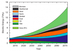
Fig. 1 Predicted production of electrical energy in the following 60 years (under assumption that the emission of the CO2 will be hold under 450ppmv).
Solar energy is high abundant source, which can be available in indirect form (wind, biomass, etc) and direct form as a solar radiation. The solar radiation reaching the Earth has power 1.8×10¹⁴ kW. 60% of this energy reaches the surface of the Earth. If only 0.1% of this energy should be with conversion efficiency of 10% transformed into the electrical energy, gained energy will be four times bigger than current electricity demand [Caillé, et al., 2007].
The current biggest drawback for wider spreading of photovoltaic (PV) is higher price of electricity produced in this way, which is in range ~4 to ~8 €/Wp [Sinke, et al., 2007]. It is not competitive with the commercial price of electricity, however, it is expected that it will be falling continuous down and will reach the value 2-4 €/Wp till 2015 [Sinke, et al., 2007]. Competitive price for the whole Europe and the so called “grid parity” is expected to attain in 2020.
The current high price of electricity from solar cells is compensated by the positive effects achieved by using of this ecologically friendly sources as well as the necessity to replace fossil fuel. Although reliable PV systems are commercially available and widely deployed, further development of PV technology is crucial to enabling PV to become a major source of electricity. In this article we will present the current status of PV technology and discuss the two mayor PV technologies with highest potential.
Current status of PV technology
Different semiconductor materials with suitable optoelectronic properties have been proposed for photovoltaic applications. Among them, silicon has been the most widely accepted and presented in current production of PV modules. The basic advantage of silicon is that it is abundant in nature and can be processed at relatively low costs, thus leading to a lowering on the energy payback time, i.e., the time needed for a photovoltaic system to produce electrical energy until it pays back the energy costs associated with its production. The silicon is presented in various crystallizations forms, where monocrystal, microcrystal and amorphous silicon are the most frequently used in photovoltaic. Current status of various photovoltaic technologies and their market share is presented in Fig. 2 [Tao, 2008].
Almost 90% share of modules production belongs to two wafer-based photovoltaic technologies based on monocrystal and microcrystal silicon. The prevalence of wafer-based silicon technology has origin in developed silicon wafers fabrication as well as a compatibility of solar cells technological processes with microelectronics industry. However, the great drawback of wafer-based silicon technology is the necessity to use silicon wafers of thickness 200-300μm, which represent a huge amount of silicon on large scale solar modules.
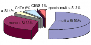
Fig. 2 The production share of PV technologies.
In recent years, the photovoltaic industry has been growing with average increase over 40% per year [Dorn, 2007]. This huge increase has made significant press on supply of silicon wafers. In 2006, for the first time, more than half of silicon production went into PV instead of computer chips. The production of silicon wafers has been not growing with the same rate as PV industry, which results in silicon wafers shortage and in increasing of their price. Today’s overall price of wafer-based silicon solar cell consists of 60% price of silicon [Rogol, 2008]. The silicon wafer shortage was a key force driving the research of technologies, which don‘t need so huge amount of expensive silicon. In following text, we will discuss two of these technologies: (i) solar cells based on thin films and (ii) solar cells with heterojunction a-Si:H/c-S (HIT – heterojunction with intrinsic thin layer).
Thin-film solar cell
The high cost of crystalline silicon wafers has led the industry to look at cheaper materials to make solar cells. One solution for this problem are thin film (TF) solar cell, which are made by deposition of one or more thin layers, mostly direct semiconductor, on a rigid substrate. The thickness range of such a layer is from a few nanometers to tens of micrometers, which leads to lower consumption of materials. Compared to traditional wafer-based crystalline silicon technologies, thin film technologies yield products of comparable performance but with significant advantages in manufacturing including fewer and automated processing steps and integrated, monolithic circuit design – no assembly of individual solar cells into final products. The deposition technologies used for fabrication of TF solar cells are carried out at lower temperatures, which decrease the overall energy budged in the process. Due to this savings of energy, the „energy payback“ time is for TF cells already around 1,5 year (for illumination in the Central Europe) [PV fact sheets, 2006].
The huge potential of TF solar cells is motivation for investment into this technology and leads to increase of its production share. The predictions say that TF solar cells production capacity will reach 1GWp in 2010 and will increase two times till 2012 [Caillé, et al., 2007].
The most common materials used in thin film based solar cells are amorphous silicon (a-Si:H) and the polycrystalline materials: cadmium telluride (CdTe) and copper indium (gallium) diselenide (CIS or CIGS). The other TF solar cells, which will be not further discussed, are organic and the dye based solar cells. According to the National Renewable Energy Laboratory institute in the USA (NREL), the promising candidates for the best price/power ration are CdTe and CIGS solar cells [Roedern, et al., 2008].
The record efficiency of CIGS is 19.2% [Green, et al., 2008], which is the maximum efficiency among all TF solar cells. Moreover, these cells can be produced by cheap roll-to-roll process. By increasing CIGS and CdTe solar cells production, however, the limit of these technologies will be attained. In Fig. 3 [Feltrin and Freundlich, 2008], the potential for solar cell production based on the assumption that 25% of the global material reserves would be available for the generation of the photovoltaic electricity is presented. Assuming an AM1.5 efficiency of 16.5%, the estimated tellurium (Te) reserves (47 ktons) limit the power production potential of CdTe photovoltaic devices to levels well below the tenth of terawatt range. Similarly, despite demonstrated AM1.5 efficiencies in excess of 19%, copper indium gallium selenide (CIGS) solar cells will merely reach the 0.02TWy level (about 100 GWp) due to the expected material shortages imposed by global indium (In) reserves (6 ktons) [Feltrin and Freundlich, 2008]. Moreover, in case of CdTe solar cell, there is always an issue with toxicity of Cadmium.
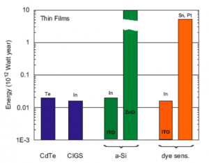
Fig. 3 Potential energy limits imposed for four different thin film photovoltaic technologies.
The potential of Dye-sensitized solar cells depends on possibility to replace indium-tin-oxide (ITO) contact with another material and can by pushed into the terawatt range. However, the dye-sensitized solar cells suffer from degradation during operation, and further research needed to be carried out to make it effective for commercial usage [Pagliaro, et. al., 2008].
As is presented in Fig. 3, the potential for energy production of amorphous silicon solar cells with ZnO contact layer is almost unlimited. Amorphous silicon technology is the oldest and best established thin-film silicon technology, which doesn’t suffer from silicon shortage. TF solar cells based on a-Si:H technology can potentially lead to low cost through lower material costs than conventional modules, but do not suffer from some critical drawbacks of other thin-film technologies, such as limited supply of basic materials or toxicity of the components.
a-Si:H and μc-Si:H silicon solar cells
Hydrogenated amorphous silicon (a-Si:H) differs from crystalline silicon by the lack of long-range order (disorder) and the high content of bonded hydrogen (typically around 10% in device-quality a-Si:H). The absence of long-range order in a-Si:H causes a relaxation in the transition rules, so that it behaves as a direct gap semiconductor with a band gap around 1.75eV [Pieters, 2008]. This behavior results in a much larger absorption in the visible part of solar spectrum, therefore much less material is needed to collect the same amount of incoming light. Active (intrinsic) layer thicknesses below 0.5μm are commonly used in a-Si:H solar cells, whereas much thicker layers (around 200μm) are required for crystalline silicon ones.
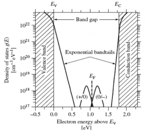
Fig. 4 Energetic distribution of density of states in band gap of amorphous silicon.
Comparing the crystalline silicon and amorphous silicon it must be emphasize the main difference in understanding of the band gap of these materials. While in case of silicon, almost no density of states is presented in the band states, a significant density of states can be observed in a-Si:H in the band gap. The presence of defects in a-Si:H has origin in two mechanisms: (i) the lack of order in the material cause a broadening of the valence and conduction bands leading to band tails, where localized energy states exist, (ii) unpassivated dangling results to defect states near the centre of the band gap. A schematic diagram of the a-Si:H density of states (DOS) is shown in Fig. 4. Band tails as well as dangling bonds act as defect states, thus leading to the presence of recombination centers and traps limiting the electrical properties of the material. The concentration of dangling bonds in common a-Si silicon is 1019 cm3 [Chopra, et al., 2004], which made this material unuseful for solar application. In order to passivate dangling bonds, approximately 10% hydrogen atoms are incorporated into the amorphous silicon resulting in decreasing of the unsaturated Si dangling bonds concentration to 1016cm3 [Chopra, et al., 2004].
Advantages of amorphous silicon PV technology are as follows the low deposition temperatures (typically 200-300°C), which permit the use of low-cost substrates; the possibility to easily integrate such modules into facades, roofs, and other structures; the relatively low production energy and low material quantities that need to be invested in the fabrication of a module; the abundance of all raw materials involved; the potential for realizing a large-scale manufacturing operation with an excellent ecological balance sheet.
One of the main disadvantages of amorphous silicon is degradation of its performance during illumination, which is called Staebler-Wronski effect (SWE) or light-induced degradation [Staebler and Wronski, 1977]. Due to the SWE effect, the electivity of the solar cell usually decreases by 15-35%. Subsequent annealing at 100-250°C can restore the original efficiency. It has become clear that the SWE is due to the creation of new defects (dangling bonds) that act as additional recombination centers.
The presented of the light-induced degradation can be superset by combining thin individual cells into a tandem and triple cells. Thinner p-i-n cells suffer less from collection problems, even if the defect density is increased by the SWE. Tandem and triple-junction cells also have the potential for a better use of the solar spectrum, provided that the band gap energies of the individual component cells can be adjusted accordingly. This can be partly achieved if amorphous silicon is used with amorphous alloys of silicon and germanium. Another possibility is the combination of amorphous silicon with microcrystalline layers to form TF hybrid solar cell called “micromorph”. Due to low band gape of microcrystal silicon (around 1,2eV), this hybrid TF solar cell has better absorption in the infrared part solar spectra and therefore offers better performance.
The major handicap of TF solar cells based on amorphous silicon is their low efficiency (Tab.1 [Green, et al., 2008; Roedern, et al., 2008]). The present laboratory record for stabilized single layer a-Si:H cell efficiency is 9.5%; actual commercial modules have stabilized efficiencies between 4% – 7%. The maximum efficiency for micromorph is 11.7%. Increased efficiency up to 13% was presented in tandem and triple solar cells [Green, et al., 2008].
| Technol. | c-Si | μc-Si:H | a-Si:H | a-Si/μc-Si |
|---|---|---|---|---|
| Lab. record | 24.7% 20.3% (multi) | 10.1% | 9.5% | 11.7% |
| Module record | 22.7% 15.3% (multi) | 8.2% | - | 10.4% |
| Module comer. | 12-19% | 6-7% | 4-7% | - |
Tab. 1 Current status of silicon solar cells.
Sanyo HIT technology
The low efficiency as well as the low stability of amorphous silicon solar cells has led to the future study of silicon wafer-based technologies, which has the ability to solve problem with silicon shortage. One of promising technology is HIT (heterojunction with intrinsic thin layer) developed by company Sanyo. Current trend in wafer-based technology is decreasing of wafer thickness. Decreasing the thickness of the wafers by 70µm brings 10-15% savings of silicon material and thus decreasing overall price. However, when the thickness of the wafer is decreased under 150µm, the high temperature processes used during fabrication have to be omitted, because they cause the wafer bending. HIT solar cell is composed of a single thin crystalline silicon wafer (~120µm) surrounded by ultra-thin intrinsic silicon layers and n-type and p-type doped amorphous silicon layers, which can be deposited using temperature below 300ºC (Fig. 5) and so can by used in processing of thin wafers. The p/n junction of the p-type substrate HIT solar cell is formed by the p-type amorphous silicon a-Si:H layer and the n-type crystalline silicon substrate. The impurity-free intrinsic amorphous silicon thin layer is inserted between the highly doped a-Si:H layer and the substrate in order to reduce recombination of charge carriers at the interface. The intrinsic amorphous layer has ability to decrease the defect density at the interface due to three orders of magnitude lower defect density presented in this layer [Jensen, et al., 2002].
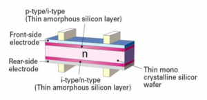
Fig. 5 SANYO HIT solar cell structure.
Fabrication process of HIT cell is simple with a relatively low manufacturing cost. Advantages of HIT solar cells are numerous [Cervantes, 2008]: good surface passivation, simple and low temperature process and high conversion efficiency. While the base material of the structure is crystalline silicon, the typical degradation (Staebler-Wronski effect) observed in amorphous silicon solar cells does not take place in HIT solar cells. This technology can be used to process very thin wafers (<100μm). In addition, HIT solar cells exhibit better temperature characteristics than conventional c-Si ones, which means more power generated in outdoor conditions for the same nominal conversion efficiency.
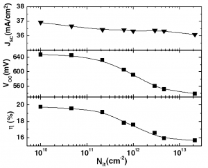
Fig. 6 Study of the influence of density of states at the interface on the performance of the cell with (p) c-Si.
The main difference between HIT and wafer-based solar cells is the presence of heterojunction in case of HIT solar cells. The presence of different conduction and valence band offsets at a-Si/c-Si heterojunction brings about the inherent superior performance of the HIT cell with the n-type silicon wafer [Stangl, et al., 2001].
The simulation study presented in Fig. 6 carried out by Maydell et al. [Maydell, et al., 2006] has shown that the quality of the a-Si:H/c-Si interface, which is related with the recombination, has serious impact on the performance of the cell. Good quality of the intrinsic a-Si:H layer as well as the interface of the a-Si:H/c-Si is one of the main challenges in order to achieve good efficiency.
This Sanyo product HIT provides industry-leading performance and value using state-of-the-art manufacturing techniques. Current world’s highest conversion efficiency level of 22.3% for HIT solar cells has been reported by Sanyo Company in 2007 [Tsunomura, et al., 2008]. This high efficiency has been mainly realized by the excellent a-Si:H/c-Si hetero-interface properties obtained by optimized surface cleaning process. The result was achieved with the open circuit voltage 0.725V, short circuit current 3.909A and fill factor 0.791.
According to the Sanyo [Tsunomura, et al., 2008], further increasing of the HIT cells performance will be achieved through improving of the a-Si:H/c-Si heterojunction, improving of the grid electrodes and reducing of the absorption in the a-Si:H and TCO layers. The improving of the heterojunction will be attainable by optimization of cleaning technology of c-Si surface before a-Si:H deposition and by lower plasma and/or thermal damage to the c-Si surface during a-Si:H, TCO and conductive electrode fabrication. In order to decrease price of fabricated modules the experiments with 70μm thick wafers are also carried out.
Conclusion
We have tried to give an up to date perspective of inorganic PV technologies. The most important material has been and still is silicon. It dominates the present world market, particularly in its crystalline and microcrystalline form but amorphous silicon is also of importance. The silicon production shortage was driving force for research others technologies. Two of them, thin film solar cells and Sanyo HIT technology were discussed here. Thin film solar cells are a promising approach for terrestrial applications and offer a wide variety of choices in terms of the device design and fabrication. Among the TF solar cells, the amorphous silicon based cells are in long-term most promising technology due to low cost processes and abundance of silicon. The lower efficiency of TF silicon solar cells is, however, disadvantage, thus another research in the field of a-Si:H solar cells need to be done. Further development will leads into decreasing of the price and improvement of performance of this kind of solar cells. For reasons stated above, it is fair to assume that silicon TF solar cells together with solar cells based on HIT technology will in the future break the current total dominance of silicon wafer-based technologies.
Acknowledgement
Presented work was supported by the MSMT CZ Grant in frame of project 1M06031
References
- Solomon, S. et al.: Climate change 2007: the physical science basis. The Intergovernmental Panel on Climate Change. Cambridge University Press. 2007. ISBN 978 0521 88009-1.
- Pearce, J.: Industrial symbiosis of very large-scale photovoltaic manufacturing. In: Renewable Energy, vol. 33, 2008, pp. 1101-1108.
- Feltrin, A., Freundlich, A.: Material considerations for terawatt level deployment of photovoltaics. In: Renewable Energy, vol. 33, 2008, pp. 180-185.
- Caillé, A. et al.: 2007 Survey of Energy Resources. London: World Energy Council. 2007. ISBN 0946121265.
- Sinke, W. et al.: A Strategic Research Agenda for Photovoltaic Solar Energy Technology 2007. The European Photovoltaic Technology Platform. Luxembourg: Office for Official Publications of the European Communities. 2007. ISBN 978-92-79-05523-2.
- Tao, M.: Inorganic Photovoltaic Solar Cells: Silicon and Beyond. In.: The Electrochemical Society Interface, 2008.
- Dorn, J.: Solar Cell Production Jumps 50 Percent in 2007. In.: Earth Policy Institute, 2007. http://www.earth-policy.org/Indicators/Solar/2007.htm
- Rogol, M.: “Refining Benchmarks and Forecasts – Rogol’s Monthly Market Commentary.” In: Photon International, 2008.
- Photovoltaic fact sheets: PV Energy Balance, 2007. www.eupvplatform.org
- Roedern, B., Ullal, H.: The Role of Polycrystalline Thin-Film PV Technologies in Competitive PV Module Markets. In: 33rd IEEE Photovoltaic Specialists Conference San Diego, 2008.
- Green, M., Emery K., Hishikawa, Y., Warta, W.: Solar Cell Efficiency Tables (Version 32). In: Progress in Photovoltaics: Research and Applications, vol. 16, 2008, pp. 435-440.
- Pagliaro, M., Palmisano, G. and Ciriminna, R.: Flexible Solar Cells. Germany: WILEY-VCH Verlag GmbH & Co. KGaA, Weinheim. 2008. ISBN 978-3-527-32375-3.
- Pieters, B.: Characterization of Thin-film silicon materials and solar cells through numerical modeling. Delft: Delft University of Technology, 2008. Dissertation thesis.
- Chopra, K., Paulson, P., Dutta, V.: Thin-Film Solar Cells: An Overview. In: Progress in Photovoltaics: Research and Applications, vol. 12, 2004, pp. 69-92.
- Staebler, D.L., Wronski, C.R.: Reversible Conductivity Changes in Discharge-Produced Amorphous Si. In: Appl. Phys. Lett., vol. 31, 1977, pp. 292-294.
- Jensen, N., Hausner, R., Bergmann, R., Werner, J., Rau, U.: Optimalization and Charakterization of Amorphous/Crystalline Silicon Heterojunction Solar Cells. In: Progress in Photovoltaics: Research and Applications, vol. 10, 2002, pp. 1-13.
- Cervantes, D. M.: Silicon heterojunction solar cells obtained by Hot-Wire CVD. Barcelona: Barcelona University of polytechnica de catalunya, 2008. Dissertation thesis.
- Stangl, R., Froitzheim, A., Elstner, L., Fuhs, W.: Amorphous/crystalline silicon heterojunction solar cells, a simulation study. In: Proceedings of 17th Photovoltaic Solar Energy, Munich 2001, pp. 1387-1390.
- Maydell, K., Korte, L., Laades, A., Stangl, R., Conrad, E., Lange, F., Schmidt, M.: Characterization and optimization of the interface quality in amorphous/crystalline silicon heterojunction solar cells. In: Journal of Non-Crystalline Solids, vol. 352, 2006, pp. 1958-1961.
- Tsunomura, Y. et al.: Twenty-two percent efficiency HIT solar cell. In: Sol. Energy Mater. Sol. Cells, 2008, Article in Press.
Co-author of this paper is L. Harmatha

