Current sensing completion detection in asynchronous circuits
12. Október, 2009, Autor článku: Nagy Lukáš, Elektrotechnika, Študentské práce
Ročník 2, číslo 10  Pridať príspevok
 In this paper, a general overview of Current Sensing Completion Detection (CSCD) method is introduced. Current sensing represents simple but effective and reliable approach to detect completion of computation in asynchronous (self-timed) systems. Two different topologies of CSCD circuits are compared and their pros and cons are presented.
Introduction
Digital circuits are divided into two basic groups. Synchronous circuits (systems) are governed by global clock signal, hence, input to each storage element has reached its final value before the next clock occurs. Therefore, behaviour of the whole circuit can be predicted exactly. On the other hand, distribution of clock signal is absolutely essential, and therefore, designing a complex synchronous circuit operating at high frequency can be difficult due to timing problems and delays.
Asynchronous systems are not controlled by a clock circuit or global clock signal, but instead they need only to wait for the signals that indicate completion of instructions and operations from previous stage. Since there is no clock signal controlling whole circuit, asynchronous systems are largely autonomous. Thus, each circuit block can operate at different speed. In synchronous circuits, no block can run faster than the clock rate. Asynchronous digital systems can dynamically adapt their operating rate to mach to silicon’s process parameters and system’s environmental conditions. This ability of adaptation allows self-timed circuits to reliably operate in a wide range of temperature, process conditions and supply voltage (M. E. Dean et al., 1991). Thus, asynchronous systems provide optimum silicon and system performance under all operating conditions. The most of digital circuits are today synchronous but self-timed asynchronous designs provide an attractive alternative. Other benefits of asynchronous circuits are: lower power dissipation for given performance and much better modularity.
Even though there is no global clock signal, we need a signal that tells us when an asynchronous circuit or its part has completed computation. Several methods of detecting the computation completion have been developed, using special coding such as 4-phase Dual-Rail, Transition Signalling or LEDR (M. E. Dean et al., 1991). These techniques require significantly larger silicon area and increase system delay. Furthermore, more variable system is working with more complex and larger completion detection circuitry, and hence, the overall system performance is degradated.
CSCD method
CSCD provides accurate completion detection even for logic functions with logic hazards and/or large capacitive loads. Signal glitches and slow transition times will not cause false completion signalling in CSCD designs, since the transient current flows any time input or output signal is not at a steady-state logic level. The goal of this method is to detect a predefined current threshold and generate a signal as soon as the transient-current flow is above this threshold level.
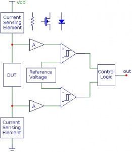
Figure 1 depicts the general block diagram of CSCD circuitry. It consists of a current sensing element (resistor, diode, transistor…) that converts the power supply current to a proportional voltage. Sense amplifier amplifies the voltage to required level. Then, a voltage comparator compares output voltage from the amplifier to a reference voltage. Outputs of the comparators are connected into the control logic block that generates a signal indicating when the self-timed circuit (DUT) has completed its computing.
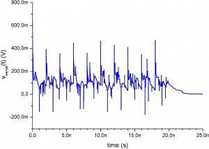
Figure 2 shows transient behaviour of voltage drop over the current sensing element. As can be noticed, when CMOS devices change their outputs due to input transitions, the transient current flowing from the power supply rapidly increases. Resulting voltage drop across the sensing device must not affect circuit’s functionality or parameters. On the other hand, this voltage has to be sufficiently high to increase signal-to-noise ratio and to be recognisable by the sense amplifier with respect to input offset.
When all the inputs and outputs of a CMOS logic block reach their final logic state, the transient supply current settles practically to zero. Most of the transient current flow is caused by charging or discharging of the capacitive loads at gate outputs. Current can flow only through the PMOS or NMOS sections of the CMOS block during most of the output transition time.
Fig. 1 General block diagram of CSCD circuit
Very important aspect of CSCD circuit is the ability to detect when the asynchronous system under test has finished computing. During design procedure of CSCD circuitry, setting the decision level must be done very carefully. Setting the decision level too early would cause false completion detection result; on the other hand, setting it too late would increase undesired delay.
Fig. 2 Example of voltage across the sensing element
Current sensor circuit
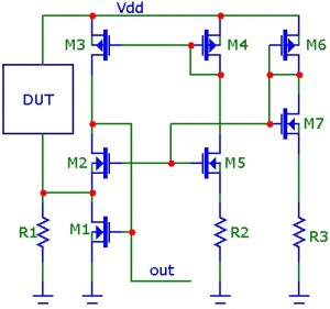
Figure 3 is shows schematic diagram of a curren sensor. Resistor R1 plays the role of a sensing element. Current flowing through this device is transformed to voltage. Transistors M6, M7 and resistor R3 create a bias voltage for the rest of the circuit. Resistor R2 sets the value of current, which is mirrored through devices M4 and M3. With current transient current consumption rising, the voltage drop across the sensing resistor increases as well. This causes decreasing voltage VGS of M2, hence, increasing potential at node where drains of M2 and M3 are connected. This node represents output of the current sensor circuit. Transistor M1 acts like an additional resistance connected to R1 in parallel. Clamping voltage over R1 is used in case when the voltage drop rises too much, and thus, causes malfunction of the self-timed circuit. With M1 connected, overall resistance decreases hence the voltage drop lowers.
However, topology described in previous paragraph cannot be used in advanced sub-90nm technologies. Monte Carlo simulations in AMS 0.35 μm process show that technology variations cause instability of so crucial bias voltage as well as circuit component mismatch. Therefore, in general, we can assume that in sub-90nm processes, results would be even worse. Inaccurate value of the bias voltage might result in false decision of computation completion. Furthermore, if we needed to design this current sensor working in weak inversion (sub-threshold region), leakage current would represent considerable issue. Absence of compensation of this problem makes this CSCD example suitable for applications in strong inversion only, and for technologies with minimal dimensions far above 90 nm.
In order to demonstrate the behaviour of a CMOS logic circuit under the transient conditions, we designed and simulated a logic circuit example. Simulations were done in Cadence environment, simulator Spectre using models of AMS 0.35 CMOS technology.
Fig. 3 Schematic diagram of CMOS current sensor
As we stated before, CMOS devices consume transient current only when they toggle logic states on their outputs. Figure 4 shows the current consumption behavior, more precisely sensed voltage over sensing element (resistor R1 in Figure 3). Asynchronous DUT used in our experiment was 4-bit carry-look-ahead adder with random input vectors [3].
Fig. 4 Sensed voltage (proportional to transient current) of a logic circuit example
Leakage current cancelling
With technology scaling that shrinks the minimal device dimensions, variations in process parameters (i.e. channel length or width, threshold voltage, subthreshold leakage current, etc.) have become major obstacles and issue for designing circuits in sub-90nm technologies [1]. Process variations and mismatch bring two major problems with design. Assumption that transistors creating a current mirror match each other perfectly may not by valid any longer. Moreover, threshold voltage of every single transistor
can vary significantly due to so-called intra-die variations.
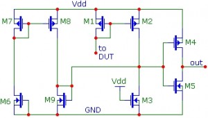
The proposed topology shown in Figure 5 depicts so-called Leakage Cancelling Current Sensor. PMOS transistor M1 with gate-drain junction shorted creates along with transistor M2 a current mirror (with 1:1 ratio). Current drawn from the power supply is mirrored into branch with transistor M3. Layout of this part has to contain dummy structures in order to provide excellent matching. Transistor M3 operates in the linear region since its gate is connected to the highest potential. Described device converts the mirrored current into proportional voltage. Transistors M4 and M5 connected together represent push-pull
inverter. M6 has its gate connected to the lowest potential that causes generation of sub-threshold leakage current, which is mirrored by transistor couple M7-M8. W/L ratio of transistor M8 is scaled to amplify the leakage current to required value. In fact, we will use parallel connection of several devices to minimize the impact of process parameters’ variations. Transistor M9 mirrors the amplified current into the branch with transistor M3. This causes a subtraction of leakage current from the total power supply current.
Fig. 5 Circuit with leakage current cancellation
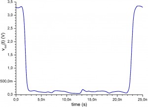
Figure 6 shows transient behaviour of the output voltage. Simulations were done with the same models and simulator as in the previous case. Leakage current in this process is not that significant in strong inversion but simulations of this CSCD cell operating in weak inversion proved inevitability of leakage current cancelling.
Fig. 6 Output voltage of the proposed circuit
Conclusion
CSCD methods is satisfactory and effective for implementing most self-timed circuits. However, in a few system environments, CSCD can present some undesirable design trade-offs or rather significant limitations. These disadvantages have to do with the static power consumption of a CSCD implementation. Sense amplifier, control logic, etc. require certain amount of static current consumption. Also delay of overall self-timed circuit slightly increases compared to one without CSCD. This is observed as a result of small voltage drop of power supply rail for logic function.
CSCD implementation does not require any special coding such as spacer tokens separating data in the data stream (needed in case of 4-phase dual-rail implementations) resulting in increased throughput. The completion detection signal generated by a CSCD implementation indicates the stability of the output signals and of the internal logic signals, allowing correct operation even with functions containing logic hazards. Another advantage is that CSCD circuit is absolutely independent on the complexity of an asynchronous system, number of its variables, and if compared to the other completion detection methods, it requires less silicon area with the same number of variables and given performance.
In future, we plan to design CSCD for asynchronous circuit in 90 nm CMOS technology. Design has to consider an option that shift of process parameters may occur. Novel approach in compensation of leakage current shall be investigated as well.
Acknowledgment
This work has been done in Center of Excelence CENAMOST (Slovak Research and Development Agency Contract No. VVCE-0049-07) with support of projects APVV-20-055405 and grant VEGA
1/0285/09.
References
- Qikai Chen, Saibal Mukhopadhyay, Hamid Mahmoodi, Kaushik Roy, “Process Variation Tolerant Online Current Monitor for Fault Immune Systems”, ECCTD, 2007
- M. E. Dean, D. L. Dill, and M. Horowitz, “Self-timed logic using current-sensing completion detection (CSCD),” in International Conference on Computer Design, 1991, pp. 187–191.
- S. Waser and M. Flynn, Topics in Arithmetic for Digital Systems Designers, Preliminary Second Edition, February 1990
Co-author of this paper is Viera Stopjaková, Slovak University of Technology, Faculty of Electrical Engineering and Information Technology, Ilkovičova 3, 812 19 Bratislava.
